
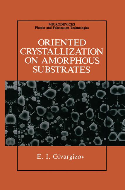
Oriented Crystallization on Amorphous Substrates
☆☆☆☆☆
(0 reviews)
Lowest price (incl. delivery)
21 474,00 JPY
Typical price3 320,74 PLN
Lowest (90 days)129,99 PLN
Offers6
Last updated1 hafta önce
Price history (90 days)
Full history
2026-08-08
2026-08-15
| Güncellenme Tarihi | Fiyat |
|---|---|
| 2026-08-08 | 129,99 |
| 2026-08-15 | 155,99 |
| Satıcı | Product price | Delivery | Toplam | Stok Durumu | Updated | |
|---|---|---|---|---|---|---|
| SP SpringerNatureLink Shop INT | 21 449,00 JPY | 25,00 JPY | 21 474,00 JPY | Mevcut | 4 gün önce | View offer |
| SP Springer Nature Author | 21 449,00 JPY | free | 21 449,00 JPY | Mevcut | 1 hafta önce | View offer |
| SP SpringerNatureLink Shop INT | 149,99 USD | free | 149,99 USD | Mevcut | 4 gün önce | View offer |
| SP SpringerNatureLink Shop INT | 169,99 USD | 15,00 USD | 184,99 USD | Mevcut | 4 gün önce | View offer |
| SP SpringerNatureLink Shop INT | 169,99 USD | free | 169,99 USD | Mevcut | 4 gün önce | View offer |
| SP SpringerNatureLink Shop INT | 177,00 EUR | 29,00 EUR | 206,00 EUR | Mevcut | 4 gün önce | View offer |
Fiyatlar ve stok durumu değişebilir. Son Güncelleme: 08.08.2026 23:33.
0,0
☆☆☆☆☆
0 reviews
5★
0%
4★
0%
3★
0%
2★
0%
1★
0%
Product reviews
No reviews yet — be the first!
Present-day scienceand technology have become increasingly based on studies and applications of thin films. This is especiallytrue of solid-state physics, semiconduc tor electronics, integrated optics, computer science, and the like. In these fields, it is necessary to use filmswith an ordered structure, especiallysingle-crystallinefilms, because physical phenomena and effects in such films are most reproducible. Also, active parts of semiconductor and other devices and circuits are created, as a rule, in single-crystal bodies. To date, single-crystallinefilms have been mainly epitaxial (or heteroepitaxial); i.e., they have been grown on a single-crystalline substrate, and principal trends, e.g., in the evolution of integrated circuits (lCs), have been based on continuing reduction in feature size and increase in the number of components per chip. However, as the size decreases into the submicrometer range, technological and physical limitations in integrated electronics become more and more severe. It is generally believed that a feature size of about 0.1um will have a crucial character. In other words, the present two-dimensional ICs are anticipated to reach their limit of minimization in the near future, and it is realized that further increase of packing density and/or functions might depend on three-dimensional integration. To solve the problem, techniques for preparation of single-crystalline films on arbitrary (including amorphous) substrates are essential.
Similar products
 50 Years of Philosophy and Medicine
from $107.30
50 Years of Philosophy and Medicine
from $107.30
 Understanding Cybersecurity Law and Digital Privacy
from $122.63
Understanding Cybersecurity Law and Digital Privacy
from $122.63
 Decisions in International Trade and Logistics
from $122.63
Decisions in International Trade and Logistics
from $122.63
 Advances in Economic Measurement
from $122.63
Advances in Economic Measurement
from $122.63
 Nanomaterials
from $137.96
Nanomaterials
from $137.96
 Sustainable Scaffolds-based Strategies in Tissue Engineering and Regenerative Medicine
from $162.87
Sustainable Scaffolds-based Strategies in Tissue Engineering and Regenerative Medicine
from $162.87
 Narratives in Educational Research
from $162.87
Narratives in Educational Research
from $162.87
 Environmental Biology of the Young Chinese Sturgeon
from $210.78
Environmental Biology of the Young Chinese Sturgeon
from $210.78