
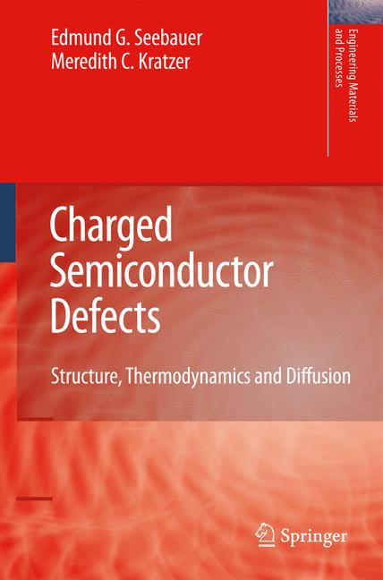
Charged Semiconductor Defects
☆☆☆☆☆
(0 opinii)
Najniższa cena (z dostawą)
21 464,00 JPY
Typowa cena2 982,30 PLN
Najniższa (90 dni)129,99 PLN
Liczba ofert6
Ostatnia aktualizacja1 tydzień temu
Historia ceny (90 dni)
Pełna historia
2026-08-08
2026-08-15
| Zaktualizowano | Cena |
|---|---|
| 2026-08-08 | 129,99 |
| 2026-08-15 | 155,99 |
| Sprzedawca | Cena produktu | Dostawa | Razem | Dostępność | Aktualizacja | |
|---|---|---|---|---|---|---|
| SP SpringerNatureLink Shop INT | 21 449,00 JPY | 15,00 JPY | 21 464,00 JPY | Dostępny | 3 dni temu | Zobacz ofertę |
| SP Springer Nature Author | 21 449,00 JPY | 0 zł | 21 449,00 JPY | Dostępny | 1 tydzień temu | Zobacz ofertę |
| SP SpringerNatureLink Shop INT | 149,99 USD | 15,00 USD | 164,99 USD | Dostępny | 3 dni temu | Zobacz ofertę |
| SP SpringerNatureLink Shop INT | 169,99 USD | 0 zł | 169,99 USD | Dostępny | 3 dni temu | Zobacz ofertę |
| SP SpringerNatureLink Shop INT | 169,99 USD | 15,00 USD | 184,99 USD | Dostępny | 3 dni temu | Zobacz ofertę |
| SP SpringerNatureLink Shop INT | 177,00 EUR | 15,00 EUR | 192,00 EUR | Dostępny | 3 dni temu | Zobacz ofertę |
Ceny i dostępność mogą ulec zmianie. Ostatnia aktualizacja: 08.08.2026 23:34.
0,0
☆☆☆☆☆
0 opinii
5★
0%
4★
0%
3★
0%
2★
0%
1★
0%
Opinie o produkcie
Brak opinii — bądź pierwszy!
Defects in semiconductors have been studied for many years, in many cases with a view toward controlling their behaviour through various forms of “defect engineering”. For example, in the bulk, charging significantly affects the total concentration of defects that are available to mediate phenomena such as solid-state diffusion. Surface defects play an important role in mediating surface mass transport during high temperature processing steps such as epitaxial film deposition, diffusional smoothing in reflow, and nanostructure formation in memory device fabrication. “Charged Defects in Semiconductors” details the current state of knowledge regarding the properties of the ionized defects that can affect the behaviour of advanced transistors, photo-active devices, catalysts, and sensors. Features: group IV, III-V, and oxide semiconductors; intrinsic and extrinsic defects; and, point defects, as well as defect pairs, complexes and clusters.
Podobne produkty
 50 Years of Philosophy and Medicine
od $107.30
50 Years of Philosophy and Medicine
od $107.30
 Understanding Cybersecurity Law and Digital Privacy
od $122.63
Understanding Cybersecurity Law and Digital Privacy
od $122.63
 Decisions in International Trade and Logistics
od $122.63
Decisions in International Trade and Logistics
od $122.63
 Advances in Economic Measurement
od $122.63
Advances in Economic Measurement
od $122.63
 Nanomaterials
od $137.96
Nanomaterials
od $137.96
 Sustainable Scaffolds-based Strategies in Tissue Engineering and Regenerative Medicine
od $162.87
Sustainable Scaffolds-based Strategies in Tissue Engineering and Regenerative Medicine
od $162.87
 Narratives in Educational Research
od $162.87
Narratives in Educational Research
od $162.87
 Environmental Biology of the Young Chinese Sturgeon
od $210.78
Environmental Biology of the Young Chinese Sturgeon
od $210.78