
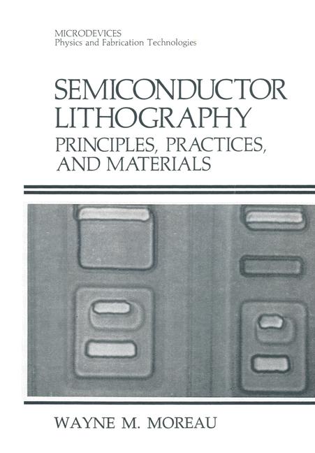
Semiconductor Lithography
☆☆☆☆☆
(0 reviews)
Lowest price (incl. delivery)
123,99 USD
Typical price2 792,86 PLN
Lowest (90 days)82,38 PLN
Offers6
Last updatedvor 5 Tagen
Price history (90 days)
Full history
2026-08-08
2026-08-15
| Aktualisiert am | Preis |
|---|---|
| 2026-08-08 | 82,38 |
| 2026-08-15 | 82,38 |
| Verkäufer | Product price | Delivery | Gesamt | Verfügbarkeit | Updated | |
|---|---|---|---|---|---|---|
| SP SpringerNatureLink Shop INT | 104,99 USD | 19,00 USD | 123,99 USD | Verfügbar | vor 5 Tagen | View offer |
| SP SpringerNatureLink Shop INT | 118,99 USD | 25,00 USD | 143,99 USD | Verfügbar | vor 4 Tagen | View offer |
| SP SpringerNatureLink Shop INT | 118,99 USD | free | 118,99 USD | Verfügbar | vor 4 Tagen | View offer |
| SP SpringerNatureLink Shop INT | 123,90 EUR | 19,00 EUR | 142,90 EUR | Verfügbar | vor 4 Tagen | View offer |
| SP SpringerNatureLink Shop INT | 21 449,00 JPY | free | 21 449,00 JPY | Verfügbar | vor 4 Tagen | View offer |
| SP Springer Nature Author | 21 449,00 JPY | 25,00 JPY | 21 474,00 JPY | Verfügbar | vor 1 Woche | View offer |
Preise und Verfügbarkeit können sich ändern. Zuletzt aktualisiert: 15.08.2026 04:14.
0,0
☆☆☆☆☆
0 reviews
5★
0%
4★
0%
3★
0%
2★
0%
1★
0%
Product reviews
No reviews yet — be the first!
Semiconductor lithography is one of the key steps in the manufacturing of integrated silicon-based circuits. In fabricating a semiconductor device such as a transistor, a series of hot processes consisting of vacuum film deposition, oxidations, and dopant implantation are all patterned into microscopic circuits by the wet processes of lithography. Lithography, as adopted by the semiconductor industry, is the process of drawing or printing the pattern of an integrated circuit in a resist material. The pattern is formed and overlayed to a previous circuit layer as many as 30 times in the manufacture of logic and memory devices. With the resist pattern acting as a mask, a permanent device structure is formed by subtractive (removal) etching or by additive deposition of metals or insulators. Each process step in lithography uses inorganic or organic materials to physically transform semiconductors of silicon, insulators of oxides, nitrides, and organic polymers, and metals, into useful electronic devices. All forms of electromagnetic radiation are used in the processing. Lithography is a mUltidisciplinary science of materials, processes, and equipment, interacting to produce three-dimensional structures. Many aspects of chemistry, electrical engineering, materials science, and physics are involved. The purpose of this book is to bring together the work of many scientists and engineers over the last 10 years and focus upon the basic resist materials, the lithographic processes, and the fundamental principles behind each lithographic process.
Similar products
 50 Years of Philosophy and Medicine
from $107.30
50 Years of Philosophy and Medicine
from $107.30
 Understanding Cybersecurity Law and Digital Privacy
from $122.63
Understanding Cybersecurity Law and Digital Privacy
from $122.63
 Decisions in International Trade and Logistics
from $122.63
Decisions in International Trade and Logistics
from $122.63
 Advances in Economic Measurement
from $122.63
Advances in Economic Measurement
from $122.63
 Nanomaterials
from $137.96
Nanomaterials
from $137.96
 Sustainable Scaffolds-based Strategies in Tissue Engineering and Regenerative Medicine
from $162.87
Sustainable Scaffolds-based Strategies in Tissue Engineering and Regenerative Medicine
from $162.87
 Narratives in Educational Research
from $162.87
Narratives in Educational Research
from $162.87
 Environmental Biology of the Young Chinese Sturgeon
from $210.78
Environmental Biology of the Young Chinese Sturgeon
from $210.78