
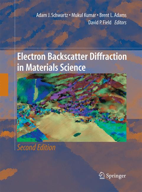
Electron Backscatter Diffraction in Materials Science
☆☆☆☆☆
(0 reviews)
Lowest price (incl. delivery)
96,40 USD
Typical price68,46 PLN
Lowest (90 days)67,40 PLN
Offers9
Last updatedvor 5 Tagen
Price history (90 days)
Full history
2026-08-08
2026-08-15
| Aktualisiert am | Preis |
|---|---|
| 2026-08-08 | 67,40 |
| 2026-08-15 | 67,40 |
| Verkäufer | Product price | Delivery | Gesamt | Verfügbarkeit | Updated | |
|---|---|---|---|---|---|---|
| SP SpringerNatureLink Shop INT | 67,40 USD | 29,00 USD | 96,40 USD | Verfügbar | vor 5 Tagen | View offer |
| SP SpringerNatureLink Shop INT | 67,40 USD | free | 67,40 USD | Verfügbar | vor 5 Tagen | View offer |
| SP SpringerNatureLink Shop INT | 67,40 EUR | 29,00 EUR | 96,40 EUR | Verfügbar | vor 5 Tagen | View offer |
| SP SpringerNatureLink Shop INT | 74,99 USD | free | 74,99 USD | Verfügbar | vor 5 Tagen | View offer |
| SP SpringerNatureLink Shop INT | 74,99 USD | 19,00 USD | 93,99 USD | Verfügbar | vor 5 Tagen | View offer |
| SP Springer Nature Author | 74,99 USD | free | 74,99 USD | Verfügbar | vor 1 Woche | View offer |
| SP SpringerNatureLink Shop INT | 299,99 USD | free | 299,99 USD | Verfügbar | vor 5 Tagen | View offer |
| SP SpringerNatureLink Shop INT | 299,99 USD | free | 299,99 USD | Verfügbar | vor 5 Tagen | View offer |
| SP SpringerNatureLink Shop INT | 329,99 EUR | free | 329,99 EUR | Verfügbar | vor 5 Tagen | View offer |
Preise und Verfügbarkeit können sich ändern. Zuletzt aktualisiert: 15.08.2026 07:33.
0,0
☆☆☆☆☆
0 reviews
5★
0%
4★
0%
3★
0%
2★
0%
1★
0%
Product reviews
No reviews yet — be the first!
Crystallographic texture or preferred orientation has long been known to strongly influence material properties. Historically, the means of obtaining such texture data has been though the use of x-ray or neutron diffraction for bulk texture measurements, or transmission electron microscopy or electron channeling for local crystallographic information. In recent years, we have seen the emergence of a new characterization technique for probing the microtexture of materials. This advance has come about primarily through the automated indexing of electron backscatter diffraction (EBSD) patterns. The first commercially available system was introduced in 1994, and since then of sales worldwide has been dramatic. This has accompanied widening the growth applicability in materials scienceproblems such as microtexture, phase identification, grain boundary character distribution, deformation microstructures, etc. and is evidence that this technique can, in some cases, replace more time-consuming transmission electron microscope (TEM) or x-ray diffraction investigations. The benefits lie in the fact that the spatial resolution on new field emission scanning electron microscopes (SEM) can approach 50 nm, but spatial extent can be as large a centimeter or greater with a computer controlled stage and montagingofthe images. Additional benefits include the relative ease and low costofattaching EBSD hardware to new or existing SEMs. Electron backscatter diffraction is also known as backscatter Kikuchi diffraction (BKD), or electron backscatter pattern technique (EBSP). Commercial names for the automation include Orientation Imaging Microscopy (OIM™) and Automated Crystal Orientation Mapping (ACOM).
Similar products
 50 Years of Philosophy and Medicine
from $107.30
50 Years of Philosophy and Medicine
from $107.30
 Understanding Cybersecurity Law and Digital Privacy
from $122.63
Understanding Cybersecurity Law and Digital Privacy
from $122.63
 Decisions in International Trade and Logistics
from $122.63
Decisions in International Trade and Logistics
from $122.63
 Advances in Economic Measurement
from $122.63
Advances in Economic Measurement
from $122.63
 Nanomaterials
from $137.96
Nanomaterials
from $137.96
 Sustainable Scaffolds-based Strategies in Tissue Engineering and Regenerative Medicine
from $162.87
Sustainable Scaffolds-based Strategies in Tissue Engineering and Regenerative Medicine
from $162.87
 Narratives in Educational Research
from $162.87
Narratives in Educational Research
from $162.87
 Environmental Biology of the Young Chinese Sturgeon
from $210.78
Environmental Biology of the Young Chinese Sturgeon
from $210.78